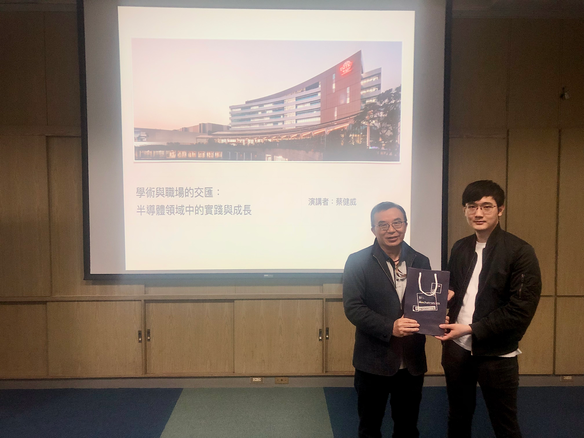
講者首先提及了台積電在半導體產業中開創的獨特商業模式,也就是對製程的專業分工。接著並介紹了晶圓的基本製造流程,涵蓋了薄膜、黃光、蝕刻、光阻去除等步驟。講者也著重分享了自身 CMP 專業的故事,從為何我們需要 CMP 到 CMP 是如何完成,講者介紹了當中使用到的研磨漿液與其化學上的功用,與說明物理研磨上使用的研磨墊,其有著不同的孔洞分佈去應對不同的情況等諸多專業細節。再來介紹了台積電的一些新技術研發到量產的流程,例如:在 R&D design house 開發的新技術,初期良率可能只有低於經濟效益的 20-30%,需要轉交給講者單位的 F12B 研發母廠來提高產品良率,之後再將成熟技術轉移到量產工廠如 18 場,以實現大規模生產。最後,講者提及了其所屬公司台積電常徵聘的各類工程師,包括製程工程師(PE)、設備工程師(EE)、良率提升工程師(YED)等等,並且分享了為何選擇台積電、與面試過程、工作時數和輪班制度、以及工作環境的實際情況,也揭示了薪資福利與公司文化。
撰寫者:大學部學生 張鈞量
The speaker began by discussing the unique business model that TSMC has pioneered in the semiconductor industry, which is the specialized division of labor in process technology. They then introduced the basic manufacturing process of wafers, covering steps such as film deposition, photolithography, etching, and photoresist removal. The speaker also shared their expertise in Chemical Mechanical Polishing (CMP), explaining why CMP is necessary, how it is performed, and detailed the use of polishing slurry and its chemical functions, as well as the polishing pads used for physical grinding, highlighting their different pore distributions to address various situations. Furthermore, the speaker described the process of developing new technologies at TSMC, from research and development in the R&D design house, where initial yields might be as low as 20-30% and not economically viable, to the improvement of product yields at the F12B pilot production plant. Mature technologies are then transferred to mass production facilities like Fab 18 to achieve large-scale production. Finally, the speaker mentioned the various types of engineers that TSMC frequently recruits, including process engineers (PE), equipment engineers (EE), and yield enhancement engineers (YED), sharing reasons for choosing TSMC, the interview process, working hours and shift systems, as well as the actual working environment. They also revealed information about salary benefits and company culture.
Author: Bachelor student, Chun-Liang ,Chang.